


Electrically pumped lasers or laser diodes based on solution-processable materials have long been desired devices for their compatibility with virtually any substrate, scalability and ease of integration with on-chip photonics and electronics. Such devices have been pursued across a wide range of materials, including polymers14,15,16, small molecules17,18, perovskites19,20 and colloidal QDs1,2,3,4,5,6,7. The last materials are especially attractive for implementing laser diodes because, as well as being compatible with inexpensive and easily scalable chemical techniques, they offer several advantages derived from a zero-dimensional character of their electronic states21,22. These include a size-tunable emission wavelength, low optical-gain thresholds and high temperature stability of lasing characteristics stemming from a wide separation between their atomic-like energy levels21,22,23.
Several challenges complicate the realization of colloidal QD laser diodes. These include extremely fast nonradiative Auger recombination of optical-gain-active multicarrier states1,8, poor stability of QD solids under high current densities required to achieve lasing9,10 and unfavourable balance between optical gain and optical losses in electroluminescent devices wherein a gain-active QD medium is a small fraction of the overall device stack comprising several optically lossy charge-transport layers11,12,13.
Here we resolve these challenges using engineered QDs with suppressed Auger recombination and a special electroluminescent-device architecture, which features a photonic waveguide consisting of a bottom distributed Bragg reflector (DBR) and a top silver (Ag) electrode. The transverse optical cavity formed by the DBR and the Ag mirror improves field confinement in the QD gain medium and simultaneously reduces optical losses in charge-conducting layers. It also facilitates the build-up of ASE owing to improved collection of spontaneous seed photons and the increased propagation path in the QD medium. As a result, we achieve large net optical gain with electrical pumping and demonstrate room-temperature ASE at the band-edge (1S) and excited-state (1P) transitions.
In this study, we use an optical gain medium based on a revised version of continuously graded QDs (cg-QDs), which are similar to our previously introduced CdSe/Cd1−xZnxSe cg-QDs9 but feature a reduced thickness of the graded layer. These ‘compact’ cg-QDs (abbreviated as ccg-QDs)13 comprise a CdSe core of 2.5 nm radius, a 2.4-nm-thick graded Cd1−xZnxSe layer and a final protective shell made of ZnSe0.5S0.5 and ZnS layers with 0.9 nm and 0.2 nm thicknesses, respectively (Fig. 1a, top-right inset and Supplementary Fig. 1). Despite its reduced thickness, the compact graded shell allows for highly effective suppression of Auger decay24, which leads to a long biexciton Auger lifetime (τXX,A = 1.9 ns) and a correspondingly high biexciton emission quantum yield of 38% (Supplementary Fig. 2). The compact graded shell also produces strong asymmetric compression of the emitting core, which increases the light-heavy hole splitting (Δlh-hh) to about 56 meV (ref. 25) (Fig. 1a). This impedes thermal depopulation of the band-edge heavy-hole state and thereby reduces the optical gain threshold7.
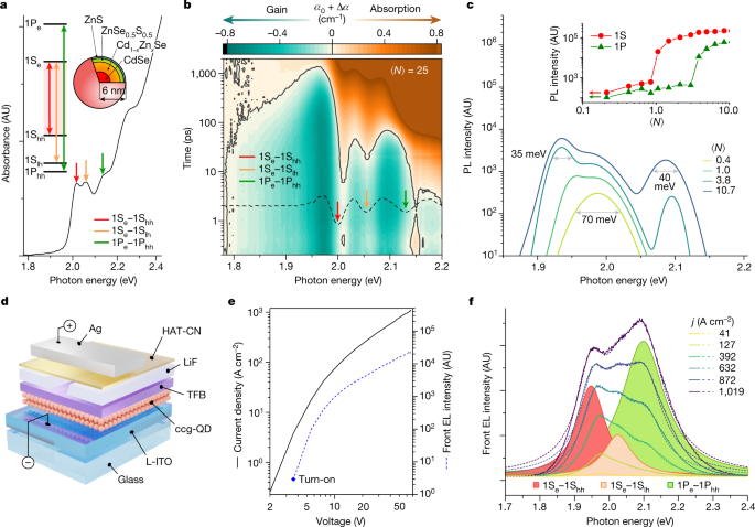
a, The ground-state absorption spectrum (α0) of the CdSe/Cd1−xZnxSe/ZnSe0.5S0.5/ZnS ccg-QDs (top-right inset). Vertical arrows mark the three lowest-energy transitions involving 1S and 1P electron and hole states (shown in the top-left inset). b, Transient absorption (TA) measurements of the ccg-QD solution sample conducted using 110-fs, 2.4-eV pump pulses with per-pulse fluence wp = 1.6 mJ cm−2 (⟨N⟩ = 25). The TA signal is presented as α(hv,t) = α0(hv) + Δα(hv,t), where α0 and α are the absorption coefficients of the unexcited and excited sample, respectively, and Δα is the pump-induced absorption change. The solid black line (α = 0) separates the regions of absorption (α > 0, brown) and optical gain (α < 0; green). The dashed black line is the second derivative of α0 (panel a). c, Pump-intensity-dependent spectra of edge-emitted photoluminescence (PL) of a 300-nm-thick ccg-QD film on a glass substrate under excitation with 110-fs, 3.6-eV pump pulses. The pump spot is shaped as a narrow 1.7-mm-long stripe orthogonal to the sample edge. The emergence of narrow peaks at 1.93 eV and 2.08 eV (full width at half maximum 35 meV and 40 meV, respectively) at higher ⟨N⟩ indicates the transition to the ASE regime. On the basis of the onset of sharp intensity growth (inset), the 1S and 1P ASE thresholds are, respectively, about 1 and about 3 excitons per dot on average. d, A device stack of the reference LED comprises an L-ITO cathode, a ccg-QD layer and TFB/HAT-CN hole transport/injection layers separated by a LiF spacer with a current-focusing aperture. The device is completed with a Ag anode prepared as a narrow strip. e, The j–V (solid black line) and EL intensity–V (dashed blue line) dependences of the reference device. f, The j-dependent EL spectra of front (surface) emission of the reference device. The EL spectrum recorded at 1,019 A cm−2 is deconvolved into three Lorentzian bands that correspond to the three ccg-QD transitions shown in a. AU, arbitrary units.
Notably, the reduced shell thickness allows for an increased QD packing density in film samples and, as a result, leads to enhanced optical gain, which spans across the 1S and 1P transitions and exhibits a wide bandwidth of about 420 meV (Fig. 1b). These properties facilitate the development of ASE, which is readily observed for optically excited ccg-QD films (Fig. 1c). The ASE occurs at both the 1S and 1P transitions and exhibits low excitation thresholds ⟨Nth,ASE⟩ ≈ 1 (1S) and 3 (1P) excitons per dot on average. On the basis of the variable stripe length (VSL) ASE measurements of a 300-nm-thick ccg-QD film, the 1S and 1P optical gain coefficients are 780 cm−1 and 890 cm−1, respectively (Supplementary Fig. 3). Owing to a near-unity mode confinement factor of the measured film, we will refer to the derived values as ‘material gain’ coefficients (Gmat,1S and Gmat,1P, respectively).
Initially, we incorporate ccg-QDs into ‘reference’ light-emitting diodes (LEDs) whose architecture is similar to that in refs. 12,13. These devices (Fig. 1d) are assembled on top of a glass substrate and comprise a ccg-QD active layer (approximately three monolayers thick) sandwiched between a bottom electrode (cathode) made of low-index indium tin oxide (L-ITO) and an organic hole-transport layer (HTL) of poly[(9,9-dioctylfluorenyl-2,7-diyl)-alt(4,4′-(N-(4-butylphenyl)))] (TFB). The L-ITO electrode is made of a mixture of standard ITO and SiO2, which reduces optical losses and enhances refractive-index contrast at the QD–cathode interface, thereby improving optical-mode confinement in the QD layer11. The TFB HTL is separated from the organic hole-injection layer (HIL) made of dipyrazino[2,3-f:2′,3′-h]quinoxaline-2,3,6,7,10,11-hexacarbonitrile (HAT-CN) by an insulating 50-nm-thick LiF spacer containing a ‘current-focusing’ 30-μm-wide slit10,12,13. The device is completed with a silver electrode (anode) prepared as a 300-μm-wide strip orthogonal to the slit in the LiF interlayer. This approach leads to two-dimensional current focusing and allows us to limit the injection area to 30 × 300 μm2. The fabricated LEDs, as well as other devices studied in this work, were characterized at room temperature in air.
In Fig. 1e,f, we show electroluminescence (EL) measurements of one of the reference LEDs excited using pulsed bias (1-μs pulse duration, 1-kHz repetition rate) with a voltage amplitude (V) up to 67 V. At the maximal voltage, the current density (j) reaches 1,019 A cm−2 (Fig. 1e), which is comparable with values realized with previous current-focusing, pulsed LEDs10. The device emission turns on at about 3 V, after which the EL intensity exhibits fast growth. The EL spectra measured at lower j peaked at 1.96 eV (1S feature), which corresponds to the band-edge 1Se–1Shh transition (Fig. 1f). As j is increased, the EL exhibits a pronounced broadening owing to increasing intensities of the higher energy bands associated with the 1Se–1Slh (2.02 eV) and the 1Pe–1Phh (2.1 eV; 1P feature) transitions (Fig. 1f and Extended Data Fig. 1a). At the highest j, the EL spectrum peaks at the position of the 1P band, which is indicative of a high per-dot excitonic number realized in these devices. In particular, on the basis of the ratio of the 1P-band and 1S-band amplitudes, the average QD excitonic occupancy ⟨N⟩ reaches roughly 7.4 (Extended Data Fig. 1b), which is higher than the optical gain threshold for both the 1S and 1P transitions (Fig. 1c).
Despite achieving population inversion, the reference devices do not exhibit ASE under electrical pumping in either front (surface) or edge emission. This indicates that the overall optical loss overwhelms optical gain generated in a thin QD medium. Photonic modelling of the reference LEDs using a finite element method confirms this assessment (Supplementary Note 1). In these devices, light amplification occurs because of optical modes guided by total internal reflection (TIR) at the L-ITO–glass interface and by the reflection at the silver mirror (Fig. 2a). Because of strong quenching by the metal layer, transverse magnetic (TM) modes experience strong attenuation, therefore, the modes preferred by ASE are of transverse electric (TE) character12,13.
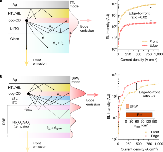
a,b Left, cross-sectional structure of the reference (a) and BRW (b) devices, along with the computed distribution of the TE modes (shown as red-shaded profiles). In the reference device, this mode is supported by TIR, whose critical angle (θc) is controlled by the refractive-index contrast at the L-ITO–glass interface (sinθc = nglass/nL-ITO). In the BRW device, the mode angle (θm = θBRW) is defined by the condition of constructive interference (Bragg condition) of reflections from different layers of the DBR. As a result, the optical-field profile exhibits an oscillatory pattern linked to the periodic structure of the DBR. Right, dependence of front-emitted and edge-emitted light intensities (yellow and red symbols, respectively) on current density for the reference (a) and BRW (b) devices. Owing to large propagation losses, the reference device radiates primarily from its front glass-cladded surface (the front-to-edge intensity ratio is about 50). By contrast, owing to reduced optical losses (inset in b, right) and strong amplification of guided light, the BRW emits more strongly from its edge (the edge-to-front intensity ratio is about 2 to 3). AU, arbitrary units.
In Fig. 2a, left, we show the computed electric-field distribution of the TE0 TIR mode. The mode confinement factor for the QD layer (ΓQD) is 0.23, which yields the maximal 1S modal gain (Gmod,1S = ΓQDGmat,1S) of about 180 cm−1. Notably, a considerable fraction of the optical mode resides in the optically lossy L-ITO electrode. This leads to a large optical loss coefficient (αloss) of about 140 cm−1 (refs. 12,13). Although it is slightly lower than Gmod,1S, light absorption in the top Ag electrode and unaccounted light scattering at imperfections within the waveguide increase the overall optical loss such that it becomes greater than modal gain, which suppresses ASE. Because of high propagation losses, the reference device exhibits very weak edge emission and radiates light primarily from the glass-cladded bottom surface such that the ratio of the surface-to-edge emission intensities is about 50 (Fig. 2a, right). Owing to the lack of light amplification, the spectrum of edge emission replicates that of surface EL at all j (Extended Data Fig. 2a).
To tackle the problem of excessive losses, we use a transverse Bragg reflector approach26 previously explored in the context of traditional laser diodes27,28. In this approach, an optical gain medium is flanked with a DBR stack on one or both sides26 (Fig. 2b, left). The resulting Bragg reflection waveguide (BRW) supports low-loss modes (Extended Data Figs. 3 and 4) that develop owing to coherent superposition of several reflections produced by the DBR structure (Fig. 2b, left). The BRW mode is favoured over the TIR modes in the case of ASE as they offer improved mode confinement within the gain-active medium and, as a result, feature reduced optical losses and enhanced net modal gain27,28. Furthermore, the BRW mode is characterized by an increased effective amplification length, as the corresponding angle of incidence (θBRW) can be considerably sharper than that in the TIR case (Fig. 2a,b, left and Extended Data Figs. 3c and 4b).
To implement a BRW waveguide, we incorporate a DBR stack made of ten pairs of Nb2O5 and SiO2 layers below the cathode (Fig. 3a and Supplementary Fig. 4). To reduce serial resistance and thereby lessen overheating at high j, we make the cathode of standard ITO rather than higher-resistivity L-ITO used in refs. 12,13. As a result, we can push the current density up to 1,933 A cm−2 (V = 53 V) without causing device breakdown (Supplementary Fig. 5). To further improve charge flow in the device, we deposit an n-type ZnO electron-transport layer (ETL) on top of the ITO cathode (Fig. 3a). The ZnO ETL is followed by the QD layer and a series of hole transport/injection layers that are similar to those of the reference LED (Fig. 3a).
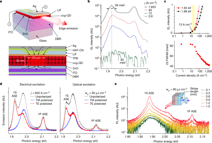
a, A BRW device is built on top of a DBR made of ten pairs of Nb2O5 and SiO2 layers. The device contains an ITO cathode, a ZnO ETL, a ccg-QD gain medium (three QD monolayers), a TFB HTL, a LiF interlayer with a current-focusing slit, a HAT-CN HIL and a strip-like Ag anode. b, Edge-emitted EL spectra of the BRW device as a function of current density tuned from 0.8 to 1,933 A cm−2. The device was excited using pulsed bias with τp = 1 μs and pulse-to-pulse separation T = 1 ms. The EL spectra show a transition from broad spontaneous emission observed at low j to sharp 1S and 1P ASE bands at high j. c, Top, the j-dependent EL intensities at the peaks of the 1S spontaneous (black) and ASE (red) bands indicate the ASE threshold jth,ASE ≈ 13 A cm−2. Bottom, the dependence of 1S emission linewidth on j indicates progressive line narrowing from 82 to 39 meV. d, Polarization characteristics of edge-emitted light of the BRW device in the case of electrical (left, j = 650 A cm−2) and optical (right, 110-fs, 3.6-eV pulses, wp = 85 μJ cm−2) excitation. Owing to strong damping of TM modes, the 1S and 1P ASE bands are not present in TM-polarized emission (blue) and exhibit nearly perfect TE polarization (red). The spontaneous 1S band is not polarized (black) and, as a result, is present in both TE-polarized and TM-polarized emission. e, The VSL measurements of the optically excited BRW device (inset) indicate the development of the 1S and 1P ASE features with increasing stripe length. These measurements used 110-fs, 3.6-eV pump pulses with wp = 90 μJ cm−2. The sharp ASE bands are similar to those observed in the EL spectra (panel b). AU, arbitrary units.
As well as improving charge transport, the ZnO layer also allows us to achieve n-doping of the active medium, as ZnO is known to facilitate electron injection into the QDs and thereby helps keep them negatively charged29,30. As shown previously, the use of charged (doped) QDs benefits lasing performance by lowering optical gain thresholds owing to partial or complete bleaching of ground-state absorption31,32,33,34,35. A potential problem of this approach is quenching of QD emission resulting from Auger recombination of charged excitonic species32,33. However, it is less of a problem with our ccg-QDs because, owing to impeded Auger decay, these QDs show high emission efficiencies for both singly and doubly negatively charged excitons (Supplementary Fig. 2).
In the fabricated structures, the bottom DBR and the top Ag mirror form a BRW. The computed electric-field distribution for the BRW mode is depicted in Fig. 2b, left. It exhibits an oscillatory pattern that reflects the periodic structure of the DBR. The main peak is centred within the QD optical gain medium, which leads to a high mode confinement factor (ΓQD = 0.2), despite the small thickness of the gain medium (approximately three ccg-QD monolayers). Notably, the BRW mode profile also features a diminished field intensity in the optical lossy ITO and ZnO layers. As a result, the overall loss coefficient is only 16 cm−1 (Extended Data Fig. 4d).
The favourable changes in the optical-field distribution have a profound effect on device EL performance. In particular, we observe a marked boost in edge emission, whose intensity becomes greater than that of surface emission by a factor of around 2 to 3 (Fig. 2b, right). This is a direct consequence of the reduced propagation losses and the emergence of the regime of ASE. The effect of ASE is pronounced in the spectra of edge-emitted EL (Fig. 3b). At low injection levels (j < 8 A cm−2), they show a weak, single-band 1S emission at 1.98 eV with an 82-meV linewidth (full width at half maximum, FWHM). At higher current densities, we observe the emergence of new narrow features whose spectral energies (1.94 and 2.09 eV) are identical to those of the 1S and 1P ASE bands in the optically excited ccg-QD film (Fig. 1c). The new bands exhibit fast superlinear growth with increasing injection level (Supplementary Fig. 6) and eventually (at j ≥ 13 A cm−2) overtake the broad 1S band (Fig. 3c, top). This is accompanied by the pronounced narrowing of the band-edge emission from 82 to 39 meV (or 23 to 13 nm; Fig. 3c, bottom). The observed j-dependent evolution of the EL spectra is very different from that for the reference LED (Fig. 1f) but very similar to the evolution of photoluminescence (PL) during the transition to ASE for the optically excited ccg-QD/glass sample (Fig. 1c). This suggests that the narrow 1S and 1P features in the edge-emitted EL are also linked to ASE.
To infer the ASE threshold, we compare the j-dependent EL signals at 1.98 eV and 1.94 eV (Fig. 3c, top), which correspond to peak energies of the spontaneous emission and ASE, respectively. Although initially the two signals grow synchronously with increasing injection level (approximately linear), they start to diverge at j > 13 A cm−2 owing to the onset of faster (superlinear) increase of the 1.94-eV EL intensity (Supplementary Fig. 6). We ascribe this behaviour to the onset of ASE and the corresponding current density to the ASE threshold (jth,ASE = 13 A cm−2). The value of jth,ASE, determined in this way, is consistent with the onset of line narrowing, characteristic of the ASE process (Fig. 3c, bottom).
The calculated ASE thresholds for our ccg-QD films depend on a charging level33 (Supplementary Note 2). For neutral QDs, jth,ASE is about 28 A cm−2 and it drops to about 26 A cm−2 and then about 15 A cm−2 for singly and doubly negatively charged QDs, respectively. The comparison of these values with jth,ASE observed experimentally suggests that, in our devices, QDs are populated with two electrons on average, which is consistent with previous studies of high-brightness cg-QD LEDs containing a ZnO ETL29.
Next, we describe evidence that the sharp 1S and 1P EL features are indeed because of photon amplification during light propagation in the BRW and not because of spectral filtering effects arising, for example, from the DBR–Ag cavity. The first piece of evidence is the close correspondence between spectral positions of the EL peaks with the optically excited 1S and 1P ASE features observed for cavity-free ccg-QD/glass samples (Fig. 1c). Second, the comparison of surface-emitted and edge-emitted EL spectra (Extended Data Fig. 2b) shows that the ASE features are spectrally distinct from the vertical cavity mode. Furthermore, the edge-emitted and surface-emitted bands show distinct behaviours as a function of j (Extended Data Fig. 5). In particular, owing to the onset of ASE, edge-emitted EL shows spectrally non-uniform intensity growth, whereas such spectral non-uniformity is absent in the surface emission.
Polarization-dependent measurements provide further evidence for the ASE regime. In particular, both sharp EL peaks observed at high j (post ASE threshold) are TE polarized and not present in TM-polarized emission (Fig. 3d and Extended Data Fig. 6). The detailed polarization-dependent measurements of the 1S and 1P EL features, ascribed to ASE, show a nearly perfect sin2α pattern, as expected for TE-polarized light (Extended Data Fig. 7; α is the angle between the polarization direction of the analyser and the vertical direction)18. This type of polarization is expected for amplified guided BRW modes, as propagation of TM modes is strongly inhibited owing to quenching by the Ag electrode12,13. Notably, the observed polarization trends are identical between the regimes of electrical and optical pumping (Fig. 3d; left and right subpanels, respectively). This is strong evidence for the ASE character of edge-emitted EL, as the ASE effect is unambiguous in optically excited edge-emitted PL spectra, as discussed below.
In Fig. 3e, we show VSL measurements of BRW structures conducted with optical excitation (see Methods). For these measurements, we prepare devices without a LiF spacer, which allows us to avoid parasitic signals from the parts of the QD layer outside the current-focusing aperture. In the VSL experiment, the pump laser beam is focused into a narrow stripe of a varied length (l), which is orthogonal to the cleaved device edge. For short stripe lengths, the edge-emitted PL is characterized by a broad spectral profile that is similar to that of EL at low injection levels (Fig. 3b,e; green lines). As l is increased, the emission intensity experiences quick growth (Supplementary Fig. 7), which is accompanied by the development of sharp peaks (Fig. 3e) whose spectral energies are in close agreement with the narrow EL features emerging at high j in electrically pumped devices (Fig. 3b, solid lines), as well as the 1S and 1P ASE bands observed for the optically excited ccg-QD/glass sample (Fig. 1c). First, these results exclude that the narrow 1S and 1P features arise from spontaneous emission of higher-order multiexcitons, as the increase in l does not affect per-pulse fluence, the quantity that controls the excitonic occupancy of the QDs. Second, these observations confirm the connection of the sharp 1S and 1P peaks to the process of stimulated emission, as the build-up of ASE does require a sufficiently long light propagation path in the gain medium approximately defined by the condition Gnetl > 1.
On the basis of the analysis of the l-dependent emission intensities, the 1S and 1P gain coefficients are 45 and 55 cm−1, respectively (Supplementary Fig. 7). These values are close to the calculated maximal net optical gain for charged QDs (Gnet = 0.5Gmod,max − αloss ≈ 64 cm−1; Supplementary Note 2), in agreement with our earlier analysis of ASE thresholds, according to which the observed gain is because of charged excitons.
The effect of ASE is also evident in the measurements of temporal coherence conducted using a Michelson interferometer. In particular, under conditions similar to those in Fig. 3d, left, the coherence time (τc) observed for the TE-polarized light is appreciably longer (by a factor of about three) than that for the TM-polarized EL (Extended Data Fig. 8). The lengthening of τc indicates a considerable contribution of ASE to the TE-polarized EL, as photon replication during light amplification enhances temporal coherence. These results are consistent with the measurements of spectrally resolved EL that indicate the dominance of ASE in the TE-polarized emission (Fig. 3d, left and Extended Data Fig. 6).
As pointed out earlier, another indication of the ASE in the BRW structures is the high brightness of edge-emitted EL (Fig. 2b, right). In the reference device, the edge signal is undetectable by the naked eye, even in the dark. By contrast, as illustrated in Fig. 4a, the light radiating from the edge of the BRW device is clearly seen even in room light, despite a very small edge-emitting area (its nominal size is approximately 9 μm2). In fact, the emission from the BRW structure can be detected and characterized with a standard power meter used to evaluate the output of commercial lasers. On the basis of such characterization, the instantaneous edge-emitted power (Pout) during the voltage pulse reaches 170 μW (j = 1,933 A cm−2); Fig. 4b (dashed blue line). A substantial role in the development of strong edge-emitted ASE is played by the BRW structure, which increases the effective amplification length and improves the collection of ‘seed’ photons produced by spontaneous emission (Supplementary Fig. 8).
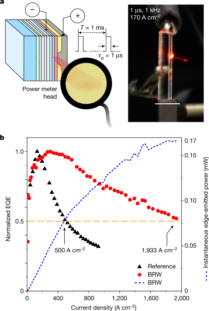
a, Left, the output of the electrically excited BRW device was characterized using a standard laser-lab power meter. The measured average power (Pav) was converted into the instantaneous output power (Pout) using Pout = (T/τp)Pav. For τp = 1 μs and T = 1 ms used in our experiments, Pout = 1,000Pav. Right, photograph of the device operating at j = 170 A cm−2 under ambient conditions in room light clearly shows edge emission that appears very bright despite the small on-time fraction (τp/T = 0.001) and the small size of the emitting spot (the nominal area is about 9 μm2). Scale bar, 10 mm. b, The dashed blue line shows the j-dependent instantaneous output power. At the maximal current density (j = 1,933 A cm−2), Pout reaches 170 μW. On the basis of the measured output power, we determine the EQE (red circles), which is compared with that of the reference device (black triangles). Owing to the efficient ASE, which leads to the increased QD emission rate and enhanced power extraction from the inverted QD medium, the EQE droop is much less pronounced in the BRW device. In particular, j½ is about four times higher than that for the reference device (1,933 versus 500 A cm−2).
The edge-emitted light exhibits a fairly tight angular distribution for out-of-plane angles (Supplementary Fig. 9a,b). It features a sharp spike (from approximately −0.2° to 0.2°), which appears on top of an asymmetric profile extending to the DBR device side. Such asymmetry is consistent with the calculated BRW mode structure (Fig. 2b, left). The angular distribution for in-plane angles is fairly flat (Supplementary Fig. 9c,d), as expected for our devices that lack angle-selection elements in the device plane.
The fabricated devices exhibit good operational stability under ambient environment. Even when the driving voltage is well above the ASE threshold, they operate for hours in the ASE regime without considerable losses in the output power. In particular, a stability test conducted at j = 120 A cm−2 (at the beginning of the test) shows that, after 2 h of continuous operation, the device still preserves around 90% of its original power (Extended Data Fig. 9). It operates in the stable ASE mode for two more hours, at which point the device finally fails.
Overall, we have fabricated 15 chips, each of which contained eight devices (120 devices in total). We observed excellent reproducibility of performance characteristics between devices on the same chip and those on different chips prepared through separate fabrication cycles. In particular, high-j EL measurements were conducted on 11 devices from different chips. All of them showed the ASE effect. As illustrated in Extended Data Fig. 10, the tested devices exhibited good consistency between their j–V (Pout–V) dependences, EL spectra, ASE thresholds and the characteristic line narrowing accompanying the transition to the ASE regime.
It is instructive to examine the external quantum efficiency (EQE) of the BRW device versus the reference LED. Because our devices lack lateral optical confinement within the QD layer and do not use any schemes for improved light outcoupling, the collected edge-emitted light is only a small fraction of the total ASE. Therefore, we will focus on the analysis of normalized EQEs as a function of current density (Fig. 4b). For the reference device, the EQE reaches its peak value at j of about 130 A cm−2, after which it shows a fast decline and drops to half of the maximal value at j = j½ = 500 A cm−2 (Fig. 4b, black triangles). This is the manifestation of a droop effect typically attributed to processes such as nonradiative Auger recombination and/or thermally induced emission quenching10,29. The BRW device also exhibits the EQE droop. However, its onset is shifted to about 300 A cm−2 and j½ is increased to about 1,930 A cm−2 (Fig. 4b, red circles). These are expected consequences of the ASE regime, which accelerates radiative recombination and thus allows it to compete more favourably with nonradiative processes.
In conclusion, we demonstrate 1S and 1P ASE with an electrically excited gain medium made of solution-cast colloidal QDs. This advance has been enabled by excellent optical-gain properties of ccg-QDs and a specially engineered device stack, which contains a low-loss photonic waveguide. This waveguide is formed by the bottom DBR and the top Ag mirror that flank the QD medium and the adjacent charge transport/injection layers. The use of the BRW allows us to shape the optical-field profile so as to reduce optical losses in charge-conducting layers and enhance mode confinement in the QD medium. These ASE diodes exhibit strong edge emission with instantaneous output power of up to 170 μW, even though they lack lateral optical confinement within the gain-active region and do not use engineered light outcoupling. The next important milestone—the realization of a QD laser oscillator—can be accomplished by supplementing the developed structures with an optical resonator implemented, for example, as either an in-plane distributed feedback grating or a Fabry–Pérot cavity formed by edge reflectors.
More News
US funders to tighten oversight of controversial ‘gain-of-function’ research
Bird flu in US cows: where will it end?
Daily briefing: Why exercise is good for us