


Advances in materials and semiconductor processes have revolutionized the design and fabrication of micro- and nano-photodetectors. But the pixels of most sensors detect only the intensity of electromagnetic waves. As a result, all phase information of the objects and diffracted light waves is lost5,6,7,8,9,10. Although intensity information alone is sufficient for conventional applications such as two-dimensional photography and microscopy imaging, this limitation hinders three-dimensional (3D) and four-dimensional imaging applications, including phase-contrast imaging, light detection and ranging, autonomous vehicles, virtual reality and space exploration11,12,13,14,15,16,17,18,19. An optical array of microlenses or photonic crystals with pixelated photodiodes is usually used to measure the light field or the distribution of light directions and thus to characterize phase information. Nevertheless, integration of these elements into complementary metal-oxide-semiconductor architectures is costly and complex4,20,21,22. Optical resonances in subwavelength semiconductor structures enable the development of angle-sensitive structures by manipulating light–matter interactions23,24,25,26,27,28. However, most of them depend on wavelength or polarization and require materials with a high refractive index29. Moreover, light-vector detection and control are at present limited to ultraviolet- and visible-light wavelengths. Although several sensors using Shack–Hartmann or Hartmann structures are capable of phase measurements in the extreme ultraviolet-light range, phase measurements of hard X-rays and gamma rays remain challenging because high-energy beams cannot be focused using conventional mirrors or microlenses30,31.
Owing to the versatility of colour encoding in data visualization, we proposed that colour-contrast encoding could be used to visualize the directions of light rays. To test our hypothesis, we selected inorganic perovskite nanocrystals because of their excellent optoelectronic properties32,33,34,35. They also demonstrate highly efficient and tunable emission with high colour saturation across the visible spectrum under X-ray or visible-light irradiation. Furthermore, Sn-based perovskite nanocrystals can have optical bandgaps that extend into the near-infrared light region36,37. A fundamental design for a 3D light-field detection involves lithographically patterning perovskite nanocrystals onto a transparent substrate (Fig. 1a). A 3D light-field sensor can then be constructed by integrating the patterned thin-film substrate with a colour charge-coupled device (CCD) that converts the angle of incident light rays into a specific colour output. The basic unit of 3D light-field sensor is a single azimuth detector comprising multicolour-emitting perovskite nanocrystals. When incident light strikes patterned nanocrystals, the azimuth angle α between the incident light and the reference plane can be detected by measuring the colour output of the basic unit (Fig. 1b). Specifically, two azimuth detectors arranged perpendicular to each other can realize 3D light-direction sensing and determine the azimuth angle φ and elevation angle θ of the incident light in spherical coordinates. To determine the absolute position of a light source, three azimuth detectors can be arranged to create a correlation among the three corresponding azimuth angles α1, α2 and α3 encoded in the colour outputs.
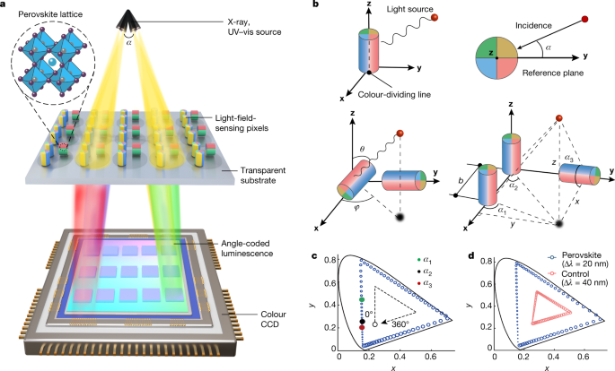
a, Design of the 3D light-field sensor on the basis of pixelated colour conversion. Light-field-sensing pixels, which consist of patterned perovskite nanocrystals on a transparent film, convert light from different directions into luminescence signals of different colours, which can be detected by a colour CCD. UV–vis, ultraviolet–visible light. b, The working principle of light-field sensing by colour conversion. The basic unit of the 3D light-field sensor is a single azimuth detector comprising multicolour-emitting perovskite nanocrystals. The colour of output luminescence depends on the angle α between the incident light and the reference plane. Two perpendicularly arranged azimuth detectors can realize 3D light-field sensing and determine the azimuth angle φ and elevation angle θ of the incident light in spherical coordinates. By arranging three azimuth detectors, correlation of the three azimuth angles α1, α2 and α3 encoded in the colour outputs of the three azimuth detectors enables detection of the absolute position (x, y, z) of a light source. c, Chromaticity responses of a single azimuth detector at light incidence from 0° to 360° relative to the reference plane. Red, green and black dots correspond to the three azimuth angles α1, α2 and α3, respectively, recorded using the three azimuth detectors shown in b. d, Chromaticity response of a single perovskite nanocrystal-based azimuth detector at light incidence from 0° to 360°, relative to the control comprising ZnS:Cu2+/Mn2+ and SrAl2O4:Eu2+/Dy3+ phosphors.
As a proof of concept, we synthesized inorganic perovskite nanocrystals (CsPbX3; X = Cl, Br or I) according to the literature36,38,39 (Supplementary Information section 1). We selected three sets of perovskite quantum dots with emissions at 445 nm, 523 nm and 652 nm to construct a single azimuth detector. When light is incident from 0° to 360° relative to the reference direction, the detected colour gamut forms a large triangle on the Commission Internationale de l’éclairage (CIE) xy chromaticity diagram (Fig. 1c). The position of the colour output on the chromaticity diagram determines the incident angle of the light and a larger triangle indicates a higher angular resolution. We found that the colour gamut of azimuth detectors made of perovskite nanocrystals forms a larger triangle in the chromaticity diagram compared with detectors made of ZnS:Cu2+/Mn2+ and SrAl2O4:Eu2+/Dy3+ phosphors (Fig. 1d). Azimuth detectors generate a higher angular resolution, because of the broader colour coverage and higher colour saturation of perovskite nanocrystals.
Single azimuth detectors with different colour gamuts produce colour plots of varying shapes (Fig. 2a). Nanocrystals with red, green and blue outputs can detect extremely small angular changes. We used this property and built a single three-colour azimuth detector on a red, green and blue sensor chip that converts incident light from 0° to 360° into different CIE XYZ tristimulus values of luminescence (Fig. 2b). The minimum detectable angular change is determined by the contrast ratio of the colour response and by the signal-to-noise ratio (SNR) of the colour sensor. Each primary colour in our tests contains 65,536 levels, which yields a detection limit of around 0.0018° angular change at a wavelength of 405 nm and a power of 8 mW (Fig. 2c).
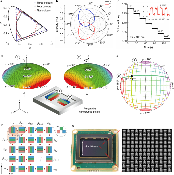
a, Chromaticity responses of single azimuthal detectors composed of three-, four- and five-colour perovskite nanocrystals as a function of the direction of incident light. b, CIE tristimulus values X, Y and Z of the output luminescence of a single azimuth detector as a function of the direction of incident light. AU, arbitrary units. c, Azimuth resolution measurement for visible light (405 nm) using a single azimuth detector, with a minimum detectable angular change of 0.0018°. Excitation (Ex) wavelength, 450 nm. d, Two types of colour map recorded from two perpendicularly aligned azimuth detectors with light incident from different azimuth angles φ and elevation angles θ. e, Contour lines extracted from the two colour maps in d. A unique incidence direction can be determined by combining the colour values from two azimuth detectors. f, Top view of the azimuthal detector arrays for imaging the 3D light direction, in which adjacent pixels of perovskite nanocrystals are aligned perpendicularly. The two detectors encircled by the ellipse can determine the angle of the beam incident on the centre point of the ellipse. Inset, side view of a patterned pixel. g, Photograph of a 3D light-field sensor fabricated by integrating the perovskite nanocrystal array into a colour CCD. Inset, a section of the microscopy image of nanocrystal-based azimuth detectors. Scale bar, 150 μm (g).
We next designed and fabricated two azimuth detectors arranged perpendicular to each other for omnidirectional light-field detection (Fig. 2d). In spherical coordinates, the azimuth angle φ and elevation angle θ for each incident beam can be calculated using the formula φ = arctan(tan α1/tan α2) and θ = arctan[(tan2 α1 + tan2 α2)1/2], respectively, where α1 and α2 are obtained from the emission colours of the two azimuth detectors (Supplementary Information sections 2–4). The two azimuth detectors yielded two types of colour map at different angles of incidence. The contours of the two colour maps in the polar plot enable specific incidence angles to be determined by combining the colour values of two azimuth detectors (Fig. 2e). We further designed azimuthal detector arrays to image the 3D light direction, in which adjacent pixels of perovskite nanocrystals were aligned perpendicular to each other (Fig. 2f). For simplicity, the angle detected by detectors parallel to the x axis is denoted by αi,j (where i and j refer to the rows and columns of the nanocrystal arrays); the angle detected by detectors parallel to the y axis is denoted by βi,j. Each of the two azimuth detectors, which are perpendicular to each other, can reconstruct the angle of the beam incident at the centre of the two pixels. For example, α1,1 and β1,2 can be used to calculate the 3D angle of the beam incident at point s11, whereas β2,1 and α1,1 can be used to calculate the 3D angle of the beam incident at point s21. Therefore, the imaging spatial resolution of the nanocrystal arrays is determined by the distance between s11 and s12. We next integrated a thin film of perovskite nanocrystal arrays into a digital camera equipped with a colour CCD (Fig. 2g). The CCD has a photosensitive area of 10 mm × 14 mm and a pixel size of 2.5 μm2 × 2.5 μm2; the pixel size of a single azimuth detector is 50 μm2 × 50 μm2.
A direct application of the light-field sensor based on pixelated perovskite nanocrystal arrays is 3D imaging and light detection and ranging (Fig. 3a). This imaging system is based on a triangulation method and consists of a multiline structured light source, two lenses for light collection and a colour CCD coated with a thin film of nanocrystal arrays. The object distance z is determined by measuring the angle of the light reflected to the nanocrystal arrays by the object—that is, a high angular resolution provides a high depth resolution. For a given pixel size (50 μm2 × 50 μm2), the theoretical depth resolution and detectable range are improved by about 10 times and 3 times, respectively, compared with conventional triangulation methods (Supplementary Information sections 5–7). To improve data accuracy, these nanocrystal arrays were calibrated first and then the imaging system was calibrated (Fig. 3b and Supplementary Information sections 8 and 9). Under light incidences from different angles θ and 𝜙, images captured using a perovskite nanocrystal array serve as a corresponding map of the colour response of each azimuth detector and the angle of incident light. To quantitatively evaluate the imaging performance of our prototype, we measured its depth accuracy as a function of scene depth and radial position within the field of view (Fig. 3c). These measurements showed an optimal depth accuracy of approximately 0.5 mm at a distance of 0.5 m, although the depth accuracy slightly decreased to approximately 1.5 mm at a distance of 2 m. Detector depth accuracy is affected by the power and angle of incident light. To ensure a high angular resolution, the power of the structured light source must be sufficient. The depth accuracy also varies depending on the intensity of the background light when the detector is used in natural-light or artificial-light conditions (Supplementary Information section 10). The dimensions of objects imaged by the light-field sensor at different distances (0.7 m and 1.5 m) are in accordance with their actual dimensions (Fig. 3d,e). Image reconstruction is also possible for objects with fine structures, such as keyboards and combs (Fig. 3f and Supplementary Information section 11). Insufficient light returned or random noise may result in undetected pixels. Moreover, we obtained 3D images of several objects of varying colours, sizes and materials at increasing depths through pixelated colour conversion (Supplementary Information section 11).
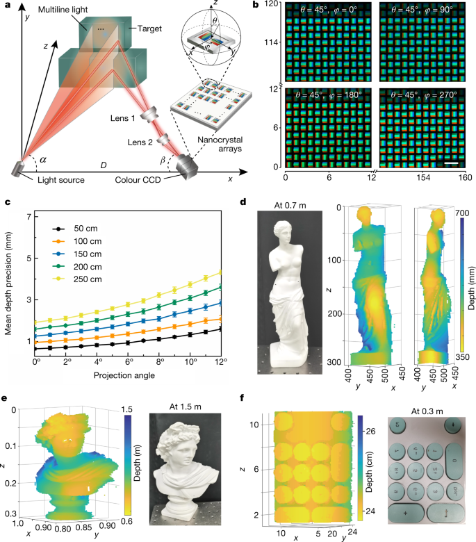
a, Schematic of the experimental set-up. Multiline structured light is incident on the object; lens 1 and lens 2 capture the reflected light and pass it to perovskite nanocrystal arrays. A colour CCD then measures the colour of each azimuth detector to calculate the corresponding distance to the scenes. b, Representative images of perovskite nanocrystal arrays with incident light from different directions. c, Mean depth precision plotted as a function of scene depth and radial position in the field of view. A movable, flat, white screen is used as the target object. Ten measurement trials were made for each projection angle and 20 measurement trials were performed for each depth. Data are mean ± s.e.m. d,e, 3D images of scenes placed at 0.7 m and 1.5 m. f, 3D depth image of a keyboard captured using the 3D light-field sensor. The colour map indicates the distance from the imaging point to the z axis at the origin (x = 0, y = 0). Scale bar, 150 μm (b).
Another important application of pixelated colour conversion is phase-contrast imaging across a broad wavelength range from X-rays to visible light (0.002–550 nm). In phase-contrast imaging with a conventional Shack–Hartmann wavefront sensor, arrays of microlenses record the angle of incidence onto a series of grid points that determine the wavefront (Fig. 4a and Supplementary Information sections 12 and 13). A nanocrystal-array-based light-field sensor can directly measure the specific angle of visible light or X-rays to reconstruct the wavefront without microlens arrays. We first characterized the diverging wavefront of a hard X-ray beam by placing the light-field sensor 14 mm from the X-ray source (Fig. 4b). The measured wavefront curvature agrees well with analytical calculations; the maximum angle measured by the light-field sensor is 40.6°. We also mapped the visible light wavefronts in the image plane when a lens was illuminated by visible light at two different field angles (Fig. 4c,d). Furthermore, phase-contrast imaging was performed using visible light on polydimethylsiloxane (PDMS) patterns and X-rays on commercial polymethylmethacrylate (PMMA) rods (Fig. 4e,f). Surface structures can be seen in greater detail by phase-contrast imaging than by absorption-contrast imaging.
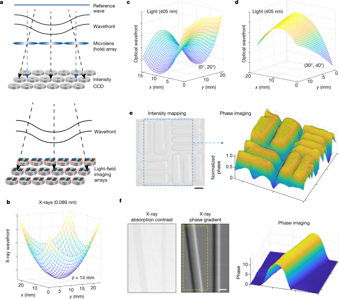
a, Principles of the Hartmann or Shack–Hartmann wavefront imaging (top) and wavefront imaging based on our 3D light-field sensor arrays (bottom). b, Measurement of a diverging wavefront of X-rays 14 mm from the X-ray source. c,d, Wavefronts measured in the image plane when a lens is illuminated by visible light at (Fx = 0°, Fy = 20°) and (Fx = 30°, Fy = 40°) field angles, respectively. Fx and Fy represent field angles in x and y directions, respectively. The focal length and aperture of the lens are 60 mm and 25.4 mm, respectively. e, Optical intensity image of a patterned PDMS substrate (left) and its phase profile (right) measured with the 3D light-field sensor. The thickness of surface structures is 0.6 mm and the wavelength of the laser is 405 nm. f, Absorption contrast image of two commercial PMMA rods (1 mm and 2 mm diameters; 50 kV X-rays) and the corresponding phase-gradient map measured using the 3D light-field sensor. Phase imaging of the yellow dashed-box region is achieved using Supplementary equation (32) of the Supplementary Information. Scale bar, 1 mm (e).
We further compared light-field sensors based on patterned nanocrystal arrays with conventional Shack–Hartmann sensors based on microlens arrays. The fabrication of nanocrystal light-field sensors is highly robust with high uniformity over a large area compared with microlens array fabrication. In our experiment, the spatial sampling density is 400 points per mm2, the angular resolution is approximately 0.015° and the dynamic angular range is greater than 80°. By contrast, Shack–Hartmann sensors with the same sampling density typically have a dynamic range of less than 2°. The nanocrystal light-field sensor can be used for a wider spectral range. However, microlens array sensors enable better visible-light collection because of their focusing effect. Compared with the spot localization method with Shack–Hartmann sensors, which is influenced by the quality of the spot and random noise, measuring the colour ratio in nanocrystal light-field sensors can be more robust.
In conclusion, we have presented a pixelated colour conversion strategy based on perovskite nanocrystal arrays for 3D light field detection, absolute spatial positioning, 3D imaging and visible light and X-ray phase-contrast imaging. With its current design, we have achieved a vector sensitivity of around 0.0018° and a wavelength response range of 0.002–550 nm. Although X-ray speckle-tracking methods can achieve an angular resolution close to nanoradians, coherent X-ray sources such as synchrotron radiation are a stringent requirement that cannot easily be met in many experimental and medical applications18,19. Further improvement in angular precision is possible by integrating high-end colour detectors. For example, a 30-bit colour display with 10-bit colour depth can yield 1.07 billion possible combinations. With advanced lithography methods and state-of-the-art processing, azimuth detector densities in excess of 104 pixels per mm2 might be achieved, which could greatly improve spatial resolution of images. At present, it is not possible to detect the light field beyond 550 nm with high angular resolution using perovskite nanocrystals. However, light-field detection and imaging through pixelated colour conversion can be readily extended to other optical materials. Sn-based perovskite nanocrystals, upconversion nanoparticles that are responsive to the near-infrared light or black phosphorus with tunable bandgaps can expand angular detection to the near-infrared, and even micrometre, wavelength range40,41. Furthermore, compared with Shack–Hartmann sensors, light-field sensors based on nanocrystal arrays can be directly integrated into the on-chip optical systems to measure wavefronts or phase. Because azimuth detectors can distinguish only the average vector direction of incident light, not the light from multiple directions like a light-field camera, our light-field sensors measure the average vector direction of light at each pixel. As with light-field cameras, nanocrystal light-field sensors must balance between angular and spatial resolution. Scanning light-field imaging systems can be coupled with nanocrystal arrays to further improve spatial resolution42. Nonetheless, the ability to image the wavefront of high-energy X-rays provides powerful solutions for optics testing and beam characterization, which can be used in applications ranging from phase-contrast imaging to gravitational-wave detection.
More News
Author Correction: Stepwise activation of a metabotropic glutamate receptor – Nature
Changing rainforest to plantations shifts tropical food webs
Streamlined skull helps foxes take a nosedive